A perfect storm of market changes is bearing down on the semiconductor industry, roiling existing business models. Long used to selling to a handful of PC and networking companies—and to shaping the path of technological development—chip makers must now work within a broader and more demanding set of ecosystems. They must create more chips for more diverse uses and contend with the increasing complexity and costs of the chips’ designs. And they must do it all while grappling with evolving economics. After years of double-digit growth, the semiconductor industry is projected to achieve a compound annual growth rate (CAGR) of just 3% to 4% from 2016 through 2020.
To succeed in this tough new landscape, chip makers must not only continue to design great products but also redesign the way they make them. They can no longer afford to go the traditional route, boosting raw compute horsepower or connectivity speed, adding memory, or creating a new capability because they can. They have to develop the right things: chips that enable the specific experiences that end users value the most. And they need to develop these products more efficiently, as well as more cost effectively, than ever before.
How can semiconductor companies do this? By embracing a highly granular, value-based approach to product design, engineering, and portfolio management. This approach, we have found, has been transformative for some companies, boosting R&D efficiencies by at least 20%. Because such gains can make all the difference when companies decide whether to enter new markets or to release new chips for new segments, they can have a direct impact on overall revenues. Indeed, the efficiency boosts can translate to an increase in TSR or market capitalization of 15% to 20%.
Chip makers that take the value-based approach aren’t just creating a future for others. They’re ensuring their own.
The Historical Approach Is History
Traditionally, semiconductor companies looked at development, whether of new products or new process nodes, through only a technical lens. They’d ask, “What is possible?” and then they’d go create it. This was the right approach when both market growth and technological innovation were experiencing large and rapid leaps. But it usually didn’t take into account what end users valued the most and how their preferences could be addressed through semiconductor products. Nor did it optimize a product portfolio to ensure that the best mix of features—for the best mix of products for the best mix of markets—were developed.
Chip makers also didn’t have to be especially proactive or aggressive to create faster, less expensive design cycles. As a result, many have yet to embrace processes that could significantly speed up development and facilitate sharing IP across products.
But today’s market is different. Three forces, in particular, are acting on and changing the environment in which semiconductor companies work. And they’re making it more essential than ever for chip makers to look at the capabilities that users value most, to allocate their resources most efficiently, and to optimize their development cycle. The three forces are:
- The Rise of the Internet of Things (IoT). A burgeoning array of connected, and often low-cost, devices are coming on the market. These products are as varied as in-car navigation units, “smart” thermostats and watches, and airborne drones. Indeed, experts estimate that by 2020, the IoT will comprise some 20 billion connected devices. And one thing is already clear: semiconductor companies will need to roll out a greater number of custom chips more frequently than ever before to cater to more devices and OEMs. A chip maker that once had 12 products in its portfolio may now have 120. And unlike PC and networking chips, these products don’t tend to be sold by the tens or hundreds of millions or at high margins.
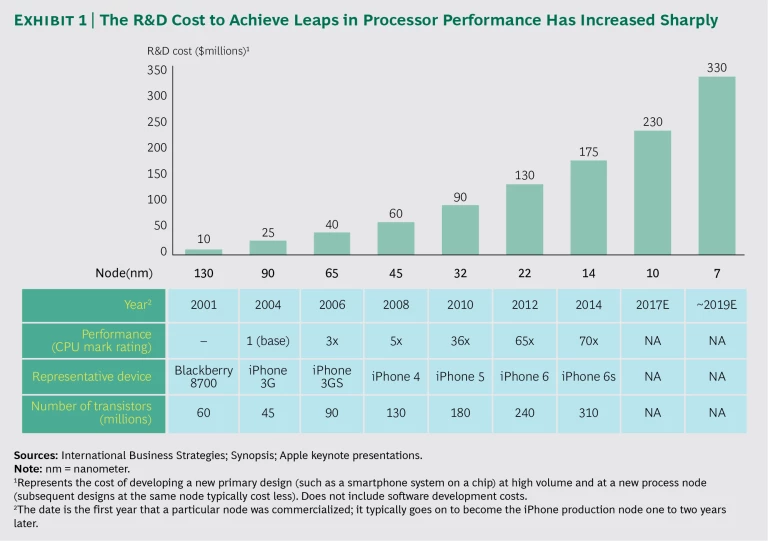
- The Increasing Cost of Innovation. The semiconductor industry, more than any other sector, has always focused intensely on R&D. In the US in 2015, R&D spending amounted to some 18% of revenues. But perhaps more telling, and sobering, are the growth rates for R&D and sales. Over the past two decades in the US, R&D spending by semiconductor companies has increased at a CAGR of 6.5%, while sales have increased by only 2.3%. This puts a strain on R&D productivity that will be exacerbated by the increasing cost of innovation. With the advent of each successive process node, the cost of developing a leading-edge design, such as a smartphone system on a chip (SoC), grows exponentially. In 2006, the cost of a new primary design at the 65 nanometer (nm) node level ran about $40 million. By 2014, at the 14 nm node level, the cost had ballooned to around $175 million, and it will go far higher with the expected arrival of 10nm and 7nm nodes. (See Exhibit 1.)
- The Shrinking Time to Market. Innovation no longer provides a long and lucrative competitive lead time. For example, wireless-chip manufacturers with advanced technology used to enjoy a market premium for two to three years before competitors came out with similar products. But with the speed of innovation declining, and strong competitors emerging, the time-to-market advantage for key technologies has now shrunk to less than six months.
Using a Value Lens
The value-based approach helps semiconductor companies not only tackle the challenges of today’s marketplace but also thrive. It enables chip makers to spend their money more wisely, build their products more efficiently, and, in the end, compete more successfully.
How does it do this? At the core of the approach is the idea that companies can and should examine a product very closely. They should analyze value creation and costs on a very detailed level, scrutinizing the different components, or IP blocks—such as memory controllers, embedded processors, interfaces, and software—within an SoC. But they should also look at individual features and the various levels at which they can perform. This kind of analysis allows a company to calculate ROI in an extremely granular way and to use that knowledge to prioritize the right components, features, and performance levels when designing the product.
One of the key benefits of this approach is that a company can tailor its business model for each subindustry that it serves. This is a critical point because, within its various segments, the semiconductor industry has always fostered a few markets in which a winner (or two) takes all.
Switching to a value lens means more than placing the right product bets, however. It also means using resources as efficiently as possible, making every dollar—and every second—count. (See Exhibit 2.)
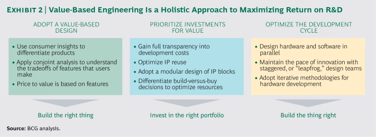
The following criteria form the three key pillars of the approach:
- Adopt a value-based design: build the right thing. Identify the products, experiences, features, and performance levels that customers value most. Then use this insight to make the right tradeoffs among design choices and to inform pricing decisions.
- Prioritize investments for value: invest in the right portfolio. Understand the true cost of each SoC component, from cores and graphics-processing units (GPUs) to third-party IP, as well as the cost of possible performance levels for different features. Correlate this with the value that the component or performance level creates to make better investment decisions, to determine whether to build or buy, and to figure out how to maximize the reuse of IP.
- Optimize the development cycle: build the thing right. Adopt emerging best practices and streamlined processes, such as staggered design teams that work in a leapfrog fashion, as well as iterative methodologies for hardware development, to build SoCs more efficiently and cost effectively.
So far, companies have employed only some parts of the value-based approach, but they have achieved positive results nevertheless. One client in the PC sector has generated $100 million annually in incremental earnings before income, taxes, depreciation, and amortization by identifying the value that consumers place on different components and using that insight to inform development, pricing, and marketing.
Mastering the full model of the value-based approach will be both a great challenge and a differentiator. Companies that can do it all will find that they have built not only the right chips but also a significant competitive edge.
Let’s take a more detailed look at the three key pillars and the steps that make them work.
Value-Based Design
For chip makers, the key to placing the right product bets is to find the sweet spot between the technical assets that they either already have or could develop and the specific needs of customers. To do this, they must have a granular understanding of both.
Semiconductor companies know what their capabilities are, but they don’t typically have a deep understanding of the value that their customers and end users place on them. Chip makers know, for example, that people want smartphones, but they don’t know what drives the decision to purchase one: What components or features do end users value most? Are they willing to pay for improved performance levels? When they buy a $600 phone instead of a $400 phone, what spurs them to spend the extra money?
This lack of granular insight means that efforts and resources are often misdirected. For example, a company might make a considerable investment in developing a state-of-the-art CPU when what end users really want is an excellent graphics engine. Complicating matters, such preferences can differ by location and by customer segment.
To figure out what triggers a sale, chip makers must break down a product into all of its individual pieces and determine the value that end users place on each one. This breakdown must be done for both the horizontal and the vertical components on a chip. (See Exhibit 3.)
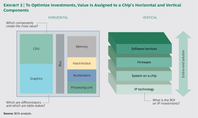
On the horizontal level are the individual components: the cores, GPU, bus, memory, accelerators, and so forth. Each of these pieces takes up space on the chip, and there is a direct correlation between that space and the cost of the product. If a company can replace a CPU with a smaller one, for instance, its manufacturing costs will go down. Perhaps even more important, the substitution frees up room for components with higher ROIs, and it may even be possible to add another USB port. If customers and end users value an extra port more than a bump in processing power, that’s a tradeoff worth making.
The same holds true on the vertical level, which includes the software layer and the firmware that links the hardware and software. For any given preference of a customer or end user—say, improved battery life—optimized software may have a greater impact on performance than greater processing speed or sharper graphics and may also improve customer satisfaction. So de-emphasizing CPU or GPU hardware development and funneling R&D resources to software that optimizes standby-mode battery usage could increase value and ROI.
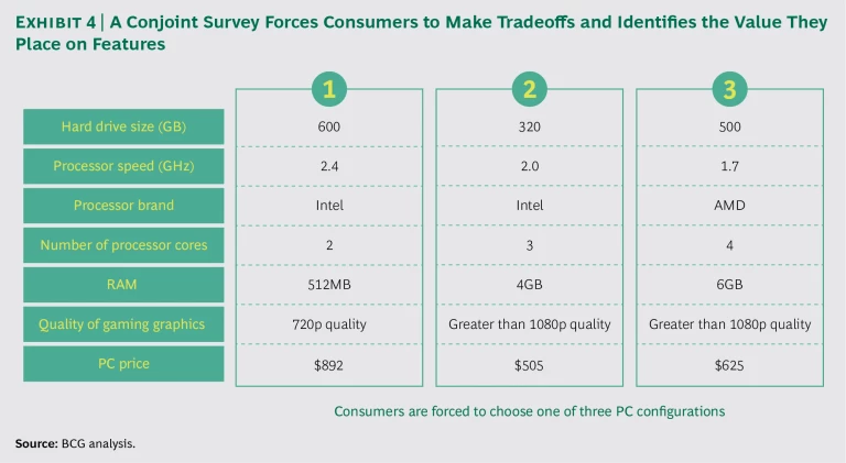
Of course, a company still must determine what matters to customers and end users, and how different performance levels, features, and experiences affect their perception of the overall value of a product. A statistical technique known as conjoint analysis can work well here. (See Exhibit 4.) Companies have used this technique, for example, to identify the relative values that consumers place on decreasing the time necessary to edit high-definition videos by 25%, 50%, and 100%.
This close examination of preferences and value enables chip makers to strike the right balance between engineering and marketing. A company can see how its R&D resources and IP can best be used to create differentiated products. And because these products specifically improve the experiences that customers and end users value most, chip makers can even capture a price premium for key differentiators.
Value-based design also gives companies a clearer sense of how products fit (or should fit) in the product portfolio. Knowing that an end user feels strongly about one particular feature or performance level is important, but chip makers are likely to find that users value a wide array of features and performance levels. The idea is to focus on those that can be incorporated into products that are particularly relevant for key customers and markets. Think of it this way: You identify two capabilities that end users deem important. One is relevant to a single product that you can sell to a few small customers in a limited market category. The other is relevant to four products that you can sell to major device manufacturers in four growing markets. Now you have a better sense of the capability and products on which to focus.
Prioritize Investments for Value
Identifying the features and performance levels that create the most value is an essential first step in making better product bets. But to truly optimize investments and wisely allocate R&D funding across components, a company must also understand costs in a very detailed way. A company able to track value and costs at the levels of features or performance, for example, would see when it is overinvesting in one component and underinvesting in another. But tracking costs like this is not easy; it requires a degree of analytical sophistication not typically seen within the industry. Project-based accounting, implemented on a very granular level, can be highly effective here and doesn’t require much change to implement.
It’s also important to evaluate build-or-buy decisions at a granular level. That’s because maximizing the ROI in innovation isn’t just about focusing on the right capabilities and performance levels. It’s also about knowing when to use third-party IP and when to develop it in-house. The key is to determine which IPs can truly help a company differentiate itself. Leveraging third-party assets for more commoditized IPs, for example, would probably make more sense than building them from scratch. Similarly, foundries make certain foundational IP and standard cells available to chip design companies. Using a foundry’s IP typically lowers R&D investment and shortens the time required to ramp up production.
Indeed, we have found that keeping the reuse of IP in mind during all discussions of assets developed in-house is very useful. The reason is simple: IP development represents a sizeable portion of a new product’s cost; reusing IP, therefore, means decreasing that cost. This is particularly significant because IP can potentially be reused along several dimensions. Subsystem blocks, such as cores and caches, for instance, can be used for different versions of a component. So a base-level CPU might contain four cores while a “pro” version might contain eight, and a “lite” version just two (in effect, a chip maker creates two additional CPUs without redesigning the cores). Meanwhile, the components themselves—such as the CPU, the GPU, and the digital signal processor—can be reused in different chip sets.
The cost savings from reusing IP can be significant. At one company, the effort required to incorporate new IP into a product was more than 15 times that needed for reusing IP. Even reusing just part of the necessary IP reduced the required effort substantially. Yet companies typically do not reuse IP in a consistent or efficient way. In our experience, companies will reuse IP about 50% to 90% of the time.
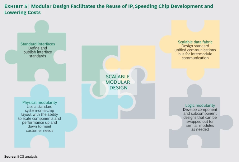
So how can chip makers facilitate IP reuse? Modular design—where components and subcomponents can be swapped out as needed and standardized interfaces and communications buses are defined—is a key enabler. (See Exhibit 5.) It helps companies to more easily incorporate both their existing IP and third-party IP, reduce SoC development time, and lower design and testing costs. More important, modular design also improves manufacturers’ ability to create custom SoCs, allowing them to simply pick and choose the most appropriate modules.
These are big upsides, but there are also a couple of downsides to modular design. SoC performance will typically be 1% to 5% lower than that of fully optimized designs. And because a standardized SoC layout is implemented to give manufacturers the ability to scale components and performance up and down as needed, the placement of components might not be optimal, increasing silicon die costs. Overall, however, the benefits of modularity far outweigh the costs.
Other practices can also help optimize IP reuse. Component design should be driven by central product teams, not just SoC teams, to avoid overcustomization for any one design. A central IP repository can make it simple for teams to find out what IP is available, while detailed documentation can make it easier for them to integrate the relevant IP into their designs. In addition, carefully managed revisions of IP and strict version control can facilitate compatibility.
Optimize the Development Cycle
The final pillar of the value-based approach is to build the product as quickly and efficiently as possible. In our work with semiconductor companies, we’ve found that abiding by the following principles can be especially helpful:
- Design software and hardware in parallel. When developing SoCs, semiconductor manufacturers traditionally focus first on designing the hardware. Only when that process is well along will they begin to work on the software. Typically, this leaves a gap of time during which the hardware is ready, but the software is still in progress. Products could get to the foundry more quickly if software development were integrated into the upfront roadmap and design process so that hardware and software could be developed simultaneously right from the start. This requires a strong capability in pre-silicon emulation, which is becoming an essential part of semiconductor design. Note, too, that a faster time to market isn’t the only benefit to be gained. The software release cycle is simplified, and the quality of releases is improved as well.
- Use leapfrog design teams. The pace of innovation and of product introductions can also be accelerated by staggering design teams. Instead of having one team develop successive generations of a core or IP block, for example, two teams could work in a leapfrog fashion. So while the first team is still working on Generation N, the second team starts to work on Generation N+1. Then when the first team is finished, it starts on Generation N+2 (with the second team still on N+1), and so on. To do this effectively, companies need to develop IP block roadmaps and standardize and reuse as many processes and tools as possible.
- Adopt iterative methodologies for hardware development. In this model, component teams deliver designs to SoC integration teams at multiple points during development instead of just once, at the end. At each of these points, the integration team analyzes and tests the component and provides feedback, which the designers factor into their next iteration. This process continues until all targets and criteria are met. Iterative development means faster time to the foundry for production—and faster time to market.
Fueled by a seemingly insatiable demand for smart and connected devices, markets are generating fresh opportunities for semiconductor companies. But seizing those opportunities requires thinking about R&D productivity and portfolio management in new and largely unfamiliar ways. Market fragmentation, lower prices, and increased competition mean that it’s no longer enough to build great products. Today’s chip makers need to build the right products the right way and at the right cost—while the clock keeps ticking.
The value-based approach helps chip makers home in on the features and performance levels that their customers and end users prize the most. It allows them to develop a holistic view of how products should fit together in their portfolios and ensures that R&D and marketing resources are allocated most effectively. This transformation isn’t simple; it requires adapting the company’s culture, incentive structures, processes, tools, and governance to the new paradigm. But the benefits are clear. In an industry where there is often no prize for coming in third (or sometimes even second), a value lens helps chip makers win.


