In 2020, we explored the economics of various types of semiconductor fabs. Our goal then was to examine the categories of capital and costs involved in building and operating typical advanced logic, advanced memory, and advanced analog chip fabs. We also investigated the role that government incentives play in the total cost of ownership (TCO)—and thus, fab competitiveness—across various regions of the world.
Since that analysis, fab economics have materially shifted. For one thing, a leading-edge advanced logic fab of the future will be at least two to three node generations beyond the ones we assessed in our earlier report. And technology advances are not all that has changed since then. There are also new supply chain and geopolitical challenges and shifting government policies and incentives. All of this has made it clear that fab economics merits a new evaluation.
This article focuses on advanced logic fabs primarily because we believe they will continue to garner the biggest investments in the coming years as the need to power all flavors of next-generation devices and equipment becomes more acute. Our analysis has led us to two fundamental conclusions. First, the cost of building and operating these fabs has risen significantly. Second, while the government incentives landscape is still evolving across multiple parts of the world, new, more aggressive financial support programs will be critical to make the economics of these massive capital-intense projects viable.
While the government incentives landscape is still evolving, more aggressive financial support programs will be critical to make the economics of today’s massive, capital-intense fab projects viable.
This research does not aim to provide a definitive number for how much these fabs should cost, nor what the incentives should be. As we will discuss in more detail, several factors that are unique to a company’s process technology, location options, design, and specification choices, among other things, can significantly sway the total cost. Consequently, this article aims to provide a framework of the considerations that should be accounted for to understand and quantify the economics of these mega projects.
Measuring the Costs of a Fab
To analyze fab economics today, we explored an advanced-logic, front-end manufacturing facility—a greenfield next-gen fab that would manufacture 2nm to sub-2nm nodes at 300-millimeter wafer size. Initial production would be scheduled for 2026. By then, we expect most companies will have undergone two major process technology advancements: First, a shift in the way individual features and transistors are fabricated on a chip; improvements are already underway that will amplify efficiency and speed, from Fin Field Effect Transistors (FinFET) to the Gate-All-Around (GAA) device structure. Second, the introduction of high numerical aperture (high-NA) extreme ultraviolet lithography (EUVL), critical for continuing to reduce the feature dimensions of the process
Upfront Costs
From a cost perspective, breaking ground on a new fab would be more expensive in the future than it was a few years ago in both upfront and ongoing expenditures. (See Exhibit 1.)
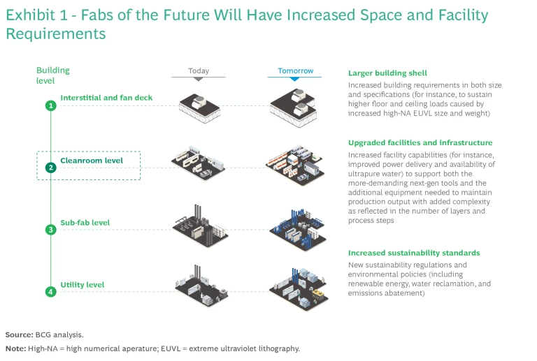
Looking at upfront costs, equipment outlays will balloon as more-advanced tools will be needed to produce next-gen nodes. (See Exhibit 2.) And construction expenditures will rise as well because more space and larger buildings will be required to house additional equipment and to maintain the necessary production volume of more numerous and complex wafer layers.
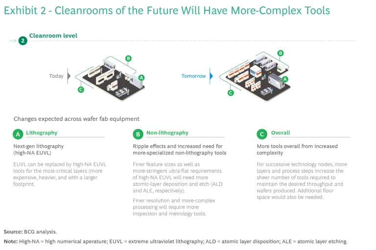
In the equipment category, the new class of EUVL machines, which will be pivotal in achieving sub-2nm nodes and are slated for scaled production around 2025, are expected to cost about twice that of today’s $150-million-plus machines. Node advancements will affect the rest of the process tools in the fab, such as those used for etching, deposition, and planarization, which will all need to be improved to meet the performance needs of the smaller feature sizes.
Historically, we have seen a 5% to 15% increase in the total number of mask layers and consequently a rise in the number of process steps involved in advancing from one major node to the next. We anticipate this cost increase trend to continue in coming years and to contribute to the need for more tools, larger cleanrooms to accommodate the extra tools, additional and more stringent building and construction standards to brace the larger fab sizes, and more sub-fab and related infrastructure to support them.
Additional cost drivers are expected to emerge as regulators and chip makers target improvements in sustainability. To meet higher sustainability benchmarks, greater use of renewable energy, water reclamation, and abatement systems for process gases will be required in new fabs.
Moreover, inflation has been elevated across the board in recent years, notably in the construction sector. For example, construction prices in the US have risen by a 6% compound annual growth rate (CAGR) since 2021, and materials costs have ballooned by 25% CAGR. (See Exhibit 3.) Building new and improved fabs requires many highly specialized capabilities, such as complex and gas delivery systems that meet micro-contamination specifications. There are very few companies in any part of the world that have the capabilities to provide these services at the right level of quality specifications.
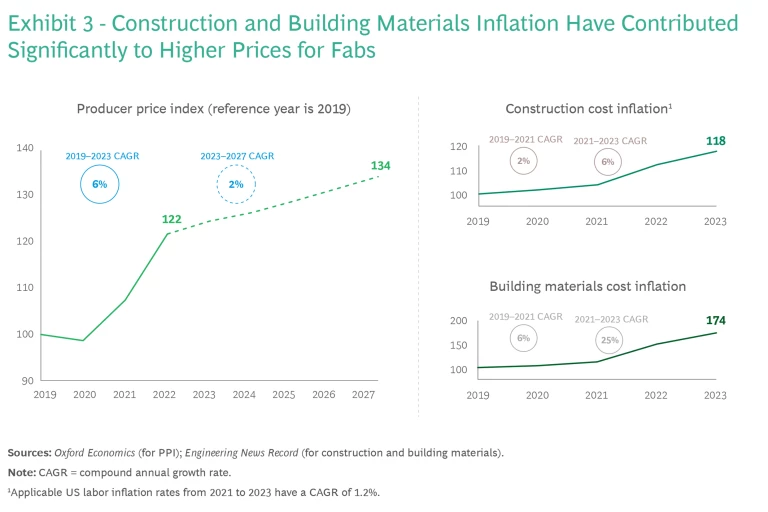
We estimate that inflation in fab construction costs will continue to remain elevated compared with broader inflation levels, primarily because without a sustained volume of new fab buildouts in recent years in many geographies—such as the US and parts of Europe—there is a limited amount of talent and expertise to support such highly specialized building programs.
Ongoing Expenses
Once the fab is in operation, there are some areas where cost increases will be keenly felt. For instance, greater amounts of materials will be needed for the additional layers and process steps in wafer production. These materials will have to be of higher quality and be more advanced than those of today to support more technologically complex manufacturing. An example of this are photoresist materials that are capable of achieving the ultra-thin films necessary for high-NA EUVL.
Perhaps surprisingly, operating labor costs are expected to be relatively stable. Leading-edge fabs are extensively automated because that approach is less likely to introduce contaminants or defects in the production process than with human intervention. As a result, staff size and responsibilities—mostly in engineering, technical, and operations functions—won’t need to change substantially.
However, maintenance costs are expected to continue to rise because more-complex and more-expensive equipment in the advanced fab will require increasingly skilled upkeep and expensive parts and components for repairs.
Utilities outlays will also be substantially affected. We expect increases beyond inflation for water, electricity, and natural gas that are in line with more process steps and layers: more steps, more consumption. Although we see continued progress among equipment manufacturers to develop more resource-efficient chip making tools, their priority remains on fab production performance—namely, throughput, critical dimensions, yields, and reliability.
Depending on where the fab is being built, local factors could impact ultimate costs, too. Among these are the availability of nearby clusters of suppliers and technicians from equipment providers, all of which could alter logistics and fab maintenance costs. Also, employee amenities that may be expected in a given region, such as recreational facilities, cafeterias, and food subsidies, could impact operating budgets. What’s more, local labor regulations, such as limits on the number of hours in a shift, may increase employee overhead expenses. The price of electricity also varies widely around the world and in some places that can make a meaningful difference in fab economics.
Taxes are also a local consideration. For example, state and local taxes in US states that already have had some degree of semiconductor industry presence (such as New York, Texas, Arizona, Ohio, and California) range from 4% to 7% and account for 1% to 3% of the ten-year TCO. Local tax structures in other parts of the world can be substantially different, and this can have an effect on the overall cost estimates for the project.
Every Fab Is Unique
These cost categories are the starting point for measuring fab economics, but they are fungible. No two fabs are the same. In fact, there are numerous approaches that semiconductor companies can take and an array of design decisions they can make during the pre-construction, construction, and operations phases that will materially alter the final cost of the fab. (See Exhibit 4.) Some of these approaches and decisions include the following:
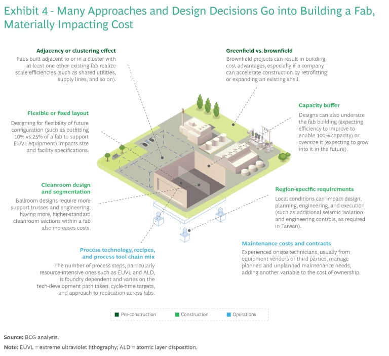
There are numerous approaches that semiconductor companies can take and an array of design decisions they can make that will materially alter the final cost of the fab.
During the Pre-Construction Phase:
- Adjacency or Clustering Effect. Fabs built next to or clustered with other chip-making facilities can deliver scale efficiencies.
- Greenfield Versus Brownfield. Brownfield projects can result in a notable advantage, saving one to two years of development simply by retrofitting or expanding an existing facility.
During the Construction Phase:
- Flexible or Fixed Layout. Designing for future configuration and use changes—for instance, outfitting 10% to 25% of the fab to support equipment with high mechanical and energy loads, such as EUVL devices—may require more-stringent specifications, such as structural steel reinforcement trusses. However, rigid approaches obviously have the downside of failing to anticipate future changes that could impact market position.
- Capacity Buffer. Decisions must be made about whether to slightly undersize the fab building with the expectation that efficiency will improve over time to enable full capacity in a smaller space, or build beyond near-term projected capacity, leaving room for growth.
- Cleanroom Design and Segmentation. Open “ballroom” designs for cleanrooms require more support trusses and engineering than do modular, mini-environment rooms, which are gaining in popularity. However, building a substantial number of higher-standard modular cleanrooms, which would protect against contaminants, may drive costs up to an unacceptable level.
- Region-Specific Requirements. Local conditions can impact design, planning, engineering, and execution. For example, additional seismic isolation and engineering controls may be needed in certain regions based on local geology to dampen possible vibrations from tremors that can disrupt wafer processing.
During the Operations Phase:
- Process Technology, Recipes, and Process Tool Chain Mix. The number of process steps, particularly those that require higher-cost, more resource-intensive equipment, such as for EUVL and atomic layer disposition (ALD), depends on the types of technologies that will be used in the fab and the building’s production complexity. Process and tool requirements will significantly impact design specifications and fab costs.
- Maintenance Costs and Contracts. Maintenance costs associated with fab equipment cover a complex landscape that stretches across all aspects of operations. These are highly specialized tools that require expertise to own, maintain in top working order, and run. Most companies must have experienced technicians (either from the equipment vendors or third parties) located on site to deal with planned and unplanned maintenance needs. The nature of these contracts can create substantial variation in the ultimate cost of ownership.
There are numerous approaches that semiconductor companies can take and an array of design decisions they can make that will materially alter the final cost of a fab.
Broadly speaking, a company’s strategic priorities and experience will impact a semiconductor fab’s budget significantly. Some companies’ business models target high fab utilization and high-volume capacity; others may be focused on on-time delivery, and still others may seek higher profit margin products even at the expense of capacity utilization. Each of these options carry distinctly different size, equipment, tools, and technology costs. Additionally, companies that are not new to fab design and development may benefit from the expertise and established resources (including specialized labor and supply-chain partners) that they have gained over time.
While all these decisions are crucial and can have a big effect on fab costs and performance, one other thing stands out in our research: fabs built by established semiconductor manufacturing companies that have access to experienced, specialized labor and partners are likely to generate the best outcomes. The experience gained from past fab builds, whether secured through in-house capabilities or strong partnerships, accelerates construction and decreases costs. By contrast, builds by either newer players or projects surrounded by unique or unfamiliar circumstances—building a first major facility in another region of the world, for instance—lack the same advantages.
At times, companies may find that they also need to account for unexpected costs. For example, as mentioned, the workers and professionals needed for fab construction are highly specialized. Companies may find that those workers are not available in sufficient numbers in the immediate area of their fab and will have to bear additional costs to support relocation of these experts from other regions.
Cost of a Hypothetical Fab
Taking the major cost drivers and underlying assumptions into consideration, we concluded that a fab completed in 2026 would carry a ten-year TCO of $35 billion to $43 billion—33% to 66% higher than today’s costs. (See Exhibit 5.)
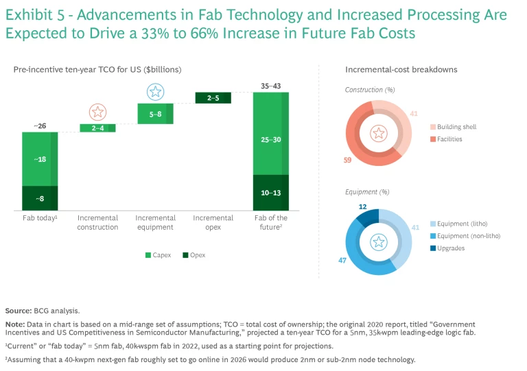
As discussed, the most critical factors propelling this increase are, first, escalating process complexity, such as increases in mask layers and a greater number of manufacturing steps, and second, an accelerated adoption rate of next-gen fab technologies—primarily high-NA EUVL. Inflation will also drive up construction and related costs. It is important to note that the wide TCO range we arrived at is extremely sensitive to shifts in any of these cost factors; for instance, if the inflation rate ends up at 2.6% rather than 4%, the cost of building a fab in 2026 could drop to as low as $37 billon.
Government Incentives Could Materially Impact Cost Outcomes
Since our analysis of fab construction three years ago, the government incentives landscape for building and operating leading-edge fab facilities has been extremely active. This is chiefly because political leaders around the world increasingly view a thriving domestic semiconductor industry and access to critical chips as essential components of economic and national security policy.
To that end, the US recently passed the CHIPS and Science Act, which provides roughly $52 billion in new funding to boost domestic research and manufacturing of semiconductors. This includes an investment tax credit of up to 25% of eligible capital expenditures (capex), a broad depreciation-eligible advanced manufacturing tax deduction that covers everything from construction to equipment. Additionally, some states offer grants to support fab construction and economic and jobs development. Some degree of long-term property tax abatement is often available as well.
Taiwan, too, is moving to solidify its global leadership position. Taiwan’s new Chips Act, which was passed in January 2023 and is in the process of being rolled out, offers investment tax credits of 25% on R&D and 5% on equipment. In addition, Taiwan industrial policy grants special benefits to research and manufacturing organizations located in science and industrial parks, including relatively low-cost access to land, water, electricity, and infrastructure, as well as the possibility of expedited approvals and the elimination of import and export duties.
South Korea is offering chip makers tax credits to cover as much as 25% of facility costs and 30% to 40% of R&D expenditures. In the wake of this program’s launch, Samsung announced a $228 billion investment over 20 years in a semiconductor cluster outside of Seoul.
Other initiatives include the European Chips Act, which is directing 22 billion Euro ($24 billion) in investments into the region’s semiconductor ecosystem; Japan’s $6.8 billion in funding for domestic semiconductor development, including a $3.5 billion subsidy for a new 10nm to 20nm fab in the Kumamoto prefecture (a joint venture of TSMC and Sony); mainland China’s ongoing consideration of new tax breaks and subsidies for the chip industry; and India’s $10 billion earmarked for chip sector expansion, which in some cases can amount to as much as 50% of project costs (since the program’s debut in 2022, Taiwanese tech leader Foxconn and US memories chip maker Micron have both indicated intent to invest in the sector in India).
Conclusion
Examining the TCO of a new fab remains a complex undertaking in today’s fast-evolving semiconductor environment. So much is changing technologically, demand is expanding rapidly, and geopolitics is disrupting chip supply chains, and all of that has made developing sufficient semiconductor manufacturing capacity an urgent priority in almost every region of the world. Understanding the underlying economics of building out chip-making facilities is critical for all stakeholders.
The right balance of incentives and support combined with R&D, innovation, and access to capital will be needed for the semiconductor industry to grow successfully. Many factors will continue to drive up the costs of these highly advanced facilities in the future, although each project will have its own unique requirements and cost considerations. The research presented here is intended to provide all interested parties with an informed perspective about the factors that most affect fab economics and the options that are available to best manage a fab’s TCO.
